
Tell me about: LiNbO3
In the "Tell me about" section, we will try to expain in a few sentences the most important aspects to fully understand the ANR-LiLit project.
On this page, you'll find an introduction to the material we will use as the piezoelectric layer of the resonating devices : lithium niobate LiNbO3
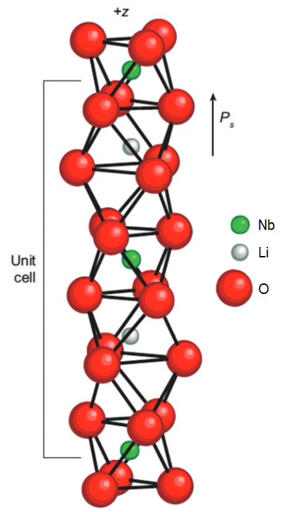
Crystal structure
Lithium niobate, formula LiNbO3, is a piezoelectric crystal belonging to the R3c (161) space group. Its structutre is represented on the left. It crystalizes in a perovskite-type strusture (ABO3), et since the crystal is non-centrosymetric, it is also ferroelectric at ambient temperature. At high temperature Tc > 1200°C, a phase transition will occur from the ferroelectrical state to the paraelectrical state due to the repositioning of the cations (Li+ and Nb5+) at the center of the oxygen octahedrons.
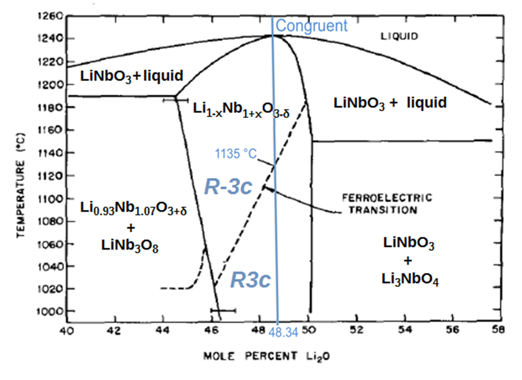 Phase diagram Li2O-Nb2O5
If we take a close look at its phase diagram (on the right), we notice that LiNbO3 exists and is stable on a large band of Lithium composition, on the left border: Li2O mol% = 46.5%, and on the right : Li2O mol% = 50%.
What's more, on this band, the crystal properties vary greatly, and with them, the performances and the working capability of the devices.
Industrial applications
LiNbO3 is an extremely important material is the fields of optics (linear and non-linear), optoelectronics and acoustics, and specifically in the telecommunications field. As a mattet of fact, its exceptionnal properties made it a staple element in resonating and filtrating devices: more than 70% of today's radiofrequency filters are based on LiNbO3 (or LiTaO3) [1].
However, filters, mainly surface acoustic wave filters (or SAW), are fabricated using LiNbO3 single crystal. Yet, to reach the required performances of the 5th Generation of telecommunications, those filters aren't suitable anymore (see Tell me about: radiofrequency filters), and we have to use another architecture that works with bulk acoustic waves (or BAW) to reach ever-increasing frequency bands. In these types of structures however, the thickness of the piezoelectric layer has to be very low.
There are two ways to reach that goal:
- The "Top-Down" approach
The idea is to glue and grind a single crystal of LiNbO3, of known composition and orientation, down to a sufficiently low thickness, tipically 100-200 nm.
Once the crystalline cut has been selected, there are multiple possible grinding/polishing techniques, but we will only focus on the most known in the semiconductor industry: the Chemical Mechanical Polishing, or CMP.
While CMP is a particularly well mastered technique [2] it exhibits limits when trying to reach very low thicknesses (< 1µm), namely the homogeneity across the whole wafer, and the brittleness of the wafers afterwards. -
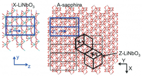
Schematic representation of LiNbO3 epitaxial growth on A sapphirre substrate [1] The "Bottom-Up" approach (ANR-LiLit project)
This time, the idea is to deposit a thin films of LiNbO3 on a selected substrate stack. If the deposition methods allows it, it is possible to have an "epitaxial" growth, i.e. oriented with respect to the most fitting(*) crystalline arrangement between the substrate and the film. ( (*)the most energetically favorable).
Some issues have to be addressed: (i) lithium stoichiometry as to be finely controlled for devices to work in the selected region, however, lithium oxide is extremely volatile ; (ii) to grow along the desired orientation may require temperatures that are uncompatible with some substrates.

[1] Bartasyte, Ausrine, et al. "Toward High‐Quality Epitaxial LiNbO3 and LiTaO3 Thin Films for Acoustic and Optical Applications." Advanced Materials Interfaces 4.8 (2017): 1600998.
[2] Sivanandini, M., et al. "Material Removal By Chemical Mechanical Polishing–A Review." International Journal of Advancements in Research & Technology, 1(5), (2012), 137-144.