The MOEMS group research activities are focused on the development of Silicon/glass technologies, following 3 main directions:
- The first topic concerns the design and implementation of on-chip optical microscopes. We propose an original integration platform, allowing the realization of compact and massively parallel microscopes with the development of basic technological building blocks (micro-optical components, MOEMS scanners). Two architectures have been demonstrated: a miniature confocal microscope and an array version of Mirau interferometer. This approach is based on the combination of silicon micromachining and micro-optics. Packaging of these microscopes is then realized by multi-wafer vertical integration techniques and/or by robotic micro-assembly on a reconfigurable microoptical silicon bench. The biomedical imaging applications are currently our main target with the implementation of two in-vivo demonstrators for OCT microscopy (optical coherence tomography): a free-space microsystem for early detection of skin diseases (European collaborative project VIAMOS) and a gastrointestinal imaging system for endomicroscopy (Labex Action: Demonstrator 4).
- The second topic concerns the realization of the European version of cesium chip-scale atomic clocks in collaboration with Time-Frequency Department of FEMTO-ST. Thanks to the European project MAC-TFC (2008-2012), led by the group, we are now the European leader in miniature cesium atomic clocks. In this framework, an important operation of industrial valorization started in December 2013, founded by DGA (HABAC project) and the BPI France program (SCP Time project).
- The third axis concerns the realization of thermal energy-harvesting microsystems based on micro Sterling engines, made in collaboration with the Energy Department of FEMTO-ST (ANR project MISTIC).
Valorization actions of our group are further strengthened by our participation to two European projects: the technology platforms ACTMOST (2010-2013) and ACTPHAST (2013-2016 Integrated European project). Since 2013, the MOEMS group is involved in the coordination and research activity of the International Collegium Smyle between FEMTO-ST and EPFL. The group is finally the contact point of FEMTO-ST for the International GDR NAMIS.
Finally, the group's research activities are closely linked to the technological platform MIMENTO, whose most important user at FEMTO-ST is the MOEMS group.
More in details:
Use of micro-opto-electro-machanical (MOEMS) technologies allows fabrication cost and power consumption reduction as well as systems and components miniaturization.
1st axis: On-chip microscopy and non-conventional micro-optical components
In the field of optical microscopy, the association of wafer-scale microfabrication techniques and MOEMS-based sensor arrays leads to an advanced miniaturization as well as a possible parallelization of measurements. This integration approach allows realizing microscopes architectures that are exceptionally compact while preserving high resolution of the measurements.
One of the challenges of the MOEMS group is to overcome the integration issues of such complicated optical microsystems by relying on multi-wafer vertical integration. Its added value lies in the possibility to build miniature microscopes or interferometers requiring 3D architectures by using free space light propagation. Two examples of such systems, developed within the MOEMS group, are the miniature confocal microscope and the Mirau micro-interferometer.
Example : Confocal microscope (frame : ANR DWST-DIS 2010-2014).
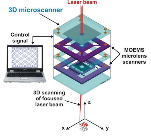
A complete architecture of an on-chip confocal microscope, vertically integrated by multi-wafer bonding, has been developed. The device is based on an illumination/detection block overhanging a 3D micro-optical scanner. The different components of the 3D microscannner are arranged in 3 functional blocks (collimation, scanning, and focusing). Scanning is achieved by MEMS actuators displacing microlenses. The complete structure is actually a stack of 7 wafers made of 3 different materials along with numerous interconnections. The 3D scanner includes two electrostatic micro-actuators: a vertical actuator (out-of-plane) and a X-Y table, each of them carrying a microlens. The challenge for the fabrication of such a system is to respect accurate alignments between the different opto-mechanical structures as well as the compatibility of each component with the bonding steps. Another challenge is to develop an efficient optical design, minimizing optical aberrations even during actuations and able to reach a high optical resolution.
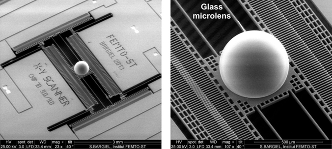 Different techniques of lens integration have been investigated: monolithic integration or assembly by robotic positioning onto the MEMS actuator membrane. Actuators displacement ranges are about 60 microns.
Generation of on-chip microscopes requires obviously the development of scientific and technological competencies regarding fabrication of both refractive and diffractive micro-optical components which are MEMS compatible.
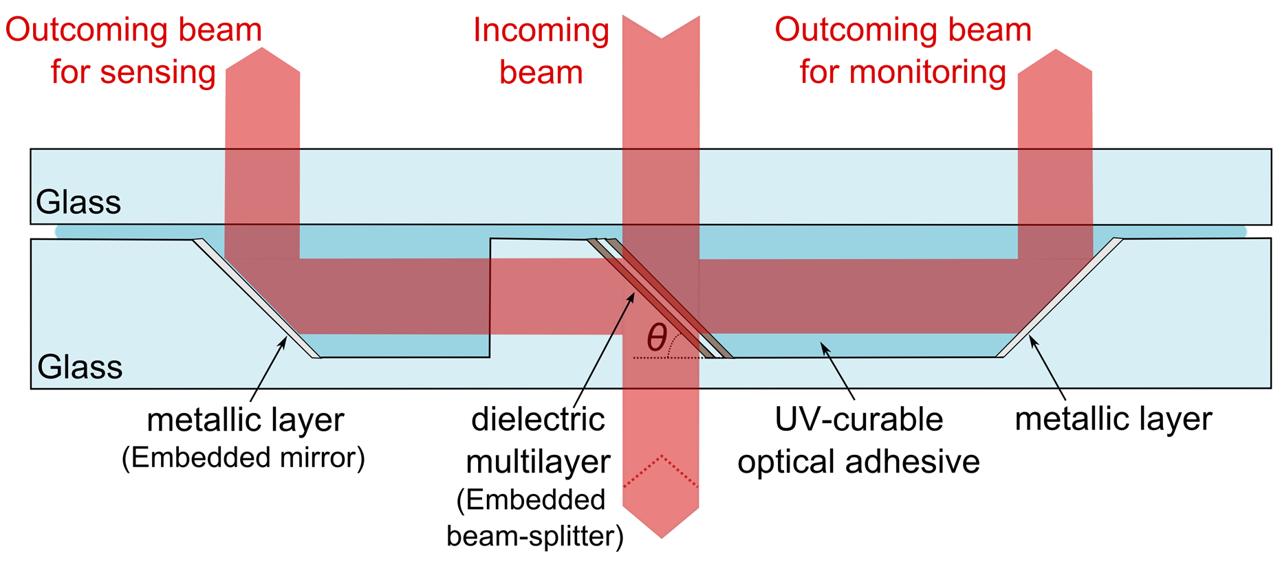
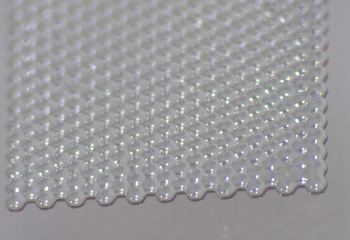
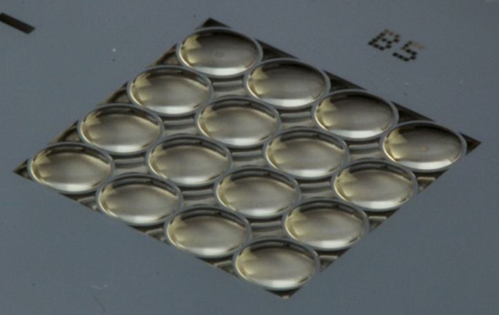
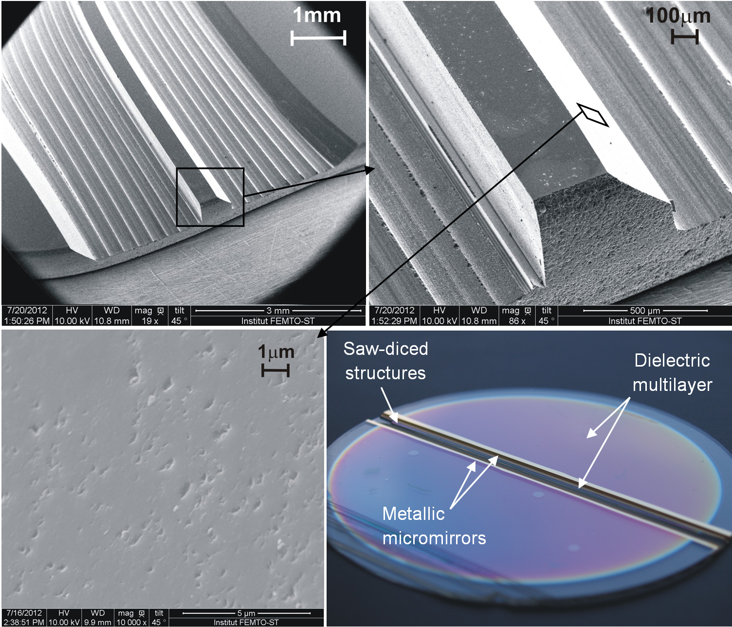 One example of generic micro-optical component for on-chip microscopy is a planar beam-splitter. In order to fabricate such miniature and thin plate (<1mm), we proposed an original concept allowing a wafer-level fabrication. The beam splitter plate is composed of two borosilicate glass wafers. One of them has 45° inclined sidewalls on which partially or totally reflecting coatings are deposited in order to route the light beam. The 45° sidewalls are made by saw dicing. The central reflector acts as a beam-splitter thanks to selective deposition of silicon-oxynitride multilayer whereas lateral reflectors are mirrors.
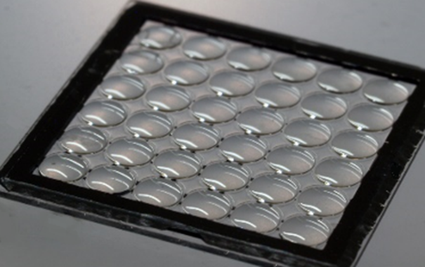
Substantial efforts are also devoted to the development of techniques for microlenses generation. In particular, one goal consists in the realization of glass microlenses which are integrated on silicon and robust against integration technologies. For instance, one of the developed techniques is based on the reflow of a glass substrate which has been previously bonded under vacuum on a silicon wafer having deep cavities. During reflow, glass moves towards the bottom of the cavity so that the convex side of the lens is generated. Whereas back side is polished until it is flat, silicon can be only partially removed on the front side to be employed as a spacer.
2nd axis: Miniature atomic clocks
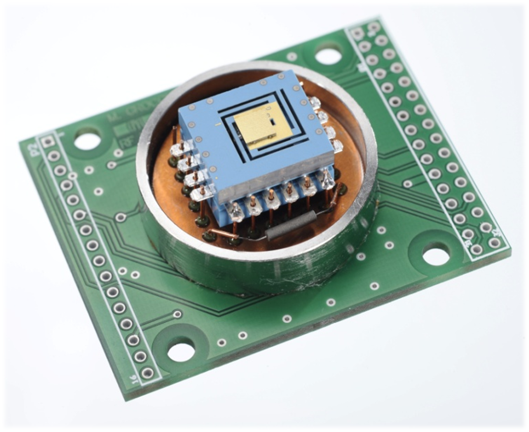 Atomic clocks are frequency and time references that allow reaching better performances in terms of frequency stability than widespread quartz oscillators. Nevertheless, volume and power consumption of atomic references are in general substantial, preventing until now their deployment into portable applications. MEMS technologies The technology of Micro Electro Mechanical Systems (MEMS), with its ability to shrink mechanical features and mechanisms down to micron scales, provides substantial size and power reduction for applications spanning wireless communications, sensors, and fluidic systems, and is now emerging to provide similar advantages for frequency and timing references. Our investigations in this field started in 2006, but really took off during the European collaborative project called MAC-TFC (2008-2012) that allowed to define and realize all the necessary technologies in order to build a complete demonstrator of a miniature atomic clock.
 The MOEMS group fabricates alkali vapor cells having well controlled pressure of buffer gases. In the so-called Dicke regime, slight and frequent alkali buffer gas collisions result in a slow diffusive motion of atoms in the cell and contribute to increase the time for alkali toms to collide against the cell walls, i.e. the clock performances: Short-term frequency stability is thus observed equal to 4x10-11 at 1 second and better than 10-11 at 1 day of integration. In this framework, we proposed an original solution based on a single buffer gaz (Neon) displaying a quadratic dependence on temperature of the Cs clock transition around a so-called inversion temperature of about 80°C.
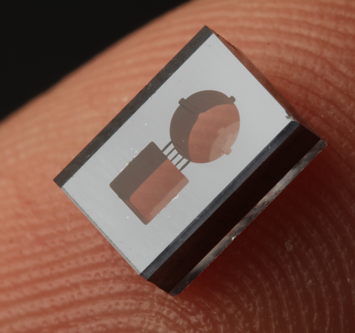
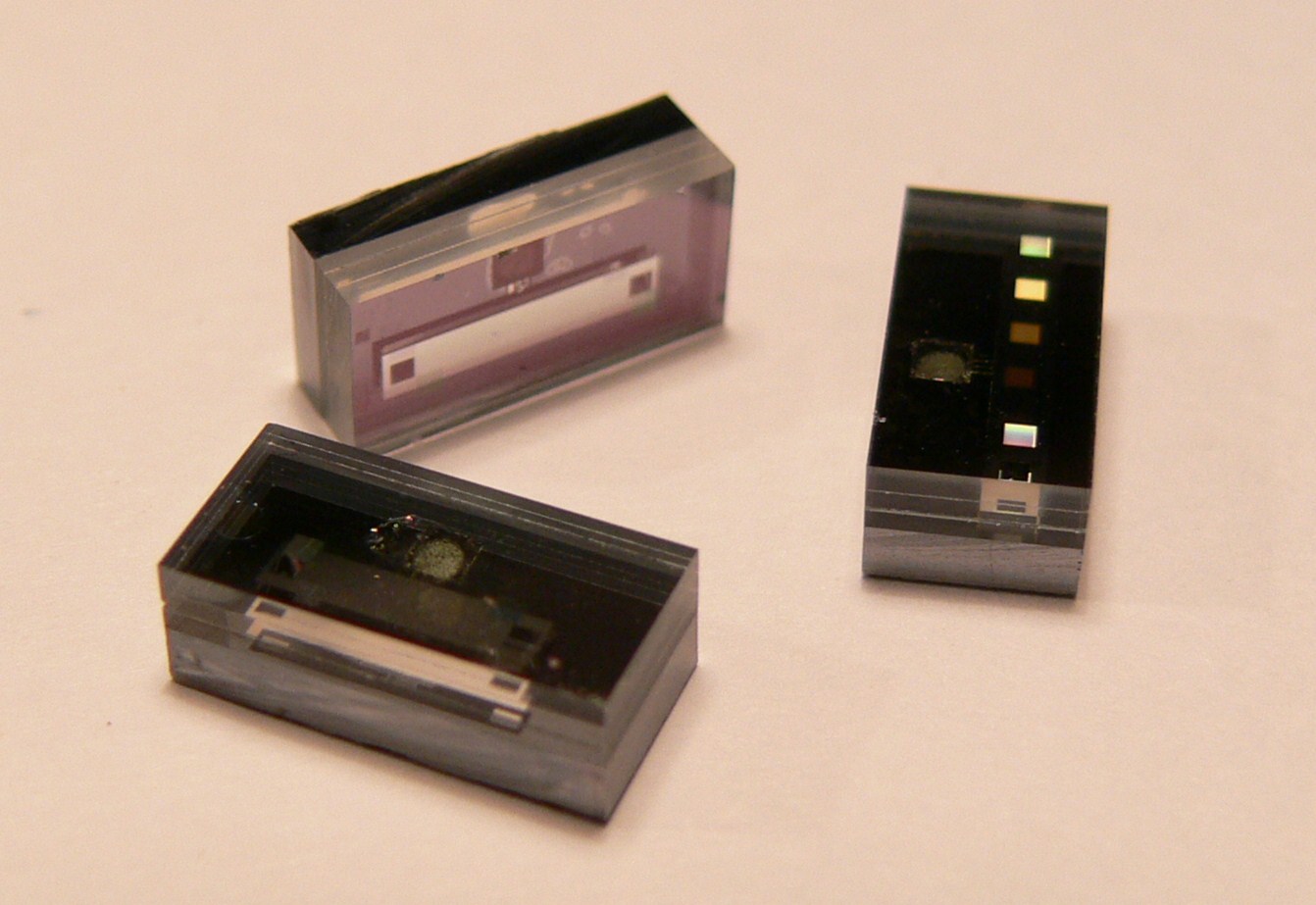 Studies on cells also concern their architecture and in particular their compliancy to wafer-scale fabrication of the entire clock. For this purpose, the MOEMS group developed a cell architecture where the optical cavity is stretched and placed along the substrate surface so that lateral dimensions can be decreased without deteriorating the performances. Such cells are equipped with diffraction gratings in order to route the optical beam inside the optical cavity without deterioration of its circular polarization state. The smaller beam section simplifies the beam shaping.
Since the end of 2013, industrial development is targeted (supported by DGA - HABAC project – and by BPI France program - SCP Time project).
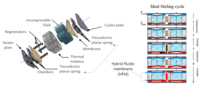
3rd axis: Microsystems for thermal energy-harvesting
The last topic of the MOEMS group concerns the development of microsystems for thermal energy harvesting.
A recent example is a thermodynamic micromachine based on Stirling cycles allowing production of electrical energy from heat. The miniature version of such a machine has not yet been realized and is a real challenge to design because of its size. The device is a stack of plates, including a warm and a cold silicon plates surrounding a thermal insulator (glass). Inside the device, a gas circulates between the cold and warm sources and is responsible for actuation of a silicone membrane oscillating as soon as a temperature difference exists. The two membranes are mechanically coupled thanks to a liquid. Membranes oscillation is subsequently transformed into electrical energy thanks to piezoelectric devices attached to the membranes.